当前位置: 阿仪网 > 光学仪器 > 光学应用 > 其它 > 深圳市蓝星宇电子科技有限公司 > 产品展示 > 光刻机&3D打印机 > 德国ParcanNano 百及纳米针尖电子束光刻系统 > ParanNano百及纳米原子力显微镜(工业型)
ParanNano百及纳米原子力显微镜(工业型)


价格:¥电议
品牌名称:$brandModel.Title型号:原产地:欧洲 更新时间:2026/10/19 9:26:31


支付方式:
- 支付宝 微信 银行转账
产品完善度: 访问次数:1714
光刻机&3D打印机
- 德国Nnaoscrib
- 德国Heidelberg
- 德国Zeiss
- 德国Eulitha
- 瑞士Swisslitho AG
- 瑞典Mycronic
- 英国Durham
- 英国Nanobean
- NanoArch
- 德国ParcanNano 百及纳米针尖电子束光刻系统
- 德国SUSS
- 美国Sonoplot
- 美国Photonics
- 美国OAI
- China
- 俄罗斯Optosystem
- 美国Coherrent
- 中科院
- 纳米压印机
- Elinoix 电子束光刻机
- 尼康Nikon光刻机
- 奥地利EVG紫外纳米压印系统
- 激光微加工设备
- 瑞士 NnaoFrazor 光刻机
- 英国AML晶圆键合机
- 德国Raith 电子束光刻机
- 德 xiton 准分子激光器
镀膜沉积机
- 德国Iplas
- 德国Sentech
- 英国HHV
- 英国Oxford
- 英国Denton
- 芬兰Picosun
- 美国Nano-master
- 法国Iplas
- 美国TED Pella
- 荷兰 TSST
- 美国Denton Vacuum
- 美Arradiance
- 法国Plassys
- 英国Oxford Vacuum
- 日立Hitachi
- 美国Neocera
- 德国MBE-Komponenten 分子束外延系统
- 英国Quorum涡轮分子泵抽真空镀膜仪
- Syskey 镀膜系统
离子刻蚀与沉积
匀胶涂覆机
半导体辅助设备
半导体微纳检测仪器
- 德国Zeiss扫描电镜
- 德国KSI超声波扫描显微镜
- 德国Mecwins扫描式激光分析仪
- 美国Nanovea三维表面形貌仪
- 德国Sentech薄膜测量仪/光伏测量仪
- 德国Klocke Nanotech 3D纳米级三维测量仪
- 德国YXLON 高分辨率X射线检测设备
- 瑞士Nanosurf 原子力显微镜
- 日本Ribm原子力显微镜
- 日本AND粒子计数器
- 日本JEOL显微镜
- 德国Bruker光谱仪/显微镜/台阶仪
- 韩国Ecopia美国MMR霍尔效应测试仪
- 探针台
- 美国Sonix超声波扫描显微镜
- 美Royce拉力性能测试及芯片拾取放置
- 美国Filmetrics膜厚测量仪
- 美国RTI自动特性图示仪
- 美国TEX Keithley半导体参数分析仪
- 美国MMR霍尔效应测量仪
- 德国neaspec纳米级红外光谱仪
- 少子寿命测试仪
- 纳米压痕仪
- FEI扫描电镜Thermo光谱仪
- XRD X射线衍射仪
- X 射线多晶衍射仪
- 日本 IAS 化学检测分析系统
- 德国IPI 水汽分析系统
- 德国PVA TePla 超声波扫描显微镜
- 德国ThetaMetrisis膜厚测量仪
实验检测仪器
- PPMS 综合物性测量系统
- MPMS3最新一代磁学测量系统
- Anasazi 科研用小型无液氦核磁共振波谱仪
- DynaCool 全新一代完全无液氦综合物性测量系统
- Oxford pulsar 实验室智能核磁共振波谱仪
- 纽迈核磁共振分业析
- Neaspec 德国真空太赫兹近场光学显微镜
- OptoCool 超精准全开放强磁场低温光学研究平台
- 德Attocube低温强磁场原子力/磁力显微镜
- Super-ME-II多铁性磁电测量系统
- Bruker 手持拉曼光谱仪
- 德国耐驰Netzsch
- 德国Moeller 测角仪
- 美Associated 耐压测试仪
- 接触角测量仪
- 氟油检漏仪
- 光学式坐标测量仪
- 光功率计
- Thorlabs傅立叶红外光谱仪
- 纳米压痕仪
- 日本Tohuko 超高灵敏度材料氧化分析仪
- 超精细多功能无液氦低温光学恒温器
- 振动样品磁强计
- 法Alyxan 高分辨质子传递反应质谱
- nanosc 高精度铁磁共振仪
- 美Microsense 磁克尔效应测量系统
- 智能型氦液化器
- 美OAI 光功率计
- 英Glovebox 手套箱
- LakeShore 振动样品磁强计
- 德国Attocube 显微镜
- 粒子碰撞噪声检测仪
- Rion 液体光学颗粒度仪
- ADLEMA 检漏机
- 德YXLON CT检测
- 电子元器件水份分析仪
紫外清洗等离子清洗机
- 美Harrich 等离子清洗机
- 德Diener 等离子清洗机
- 德PVA Tepla 微波等离子清洗机
- 美Nano-master 晶圆清洗机
- 美国Jelight UV清洗机
- 日本SEN 紫外UV清洗机UV灯
- 蓝星宇UV清洗机
- SAMCO紫外臭氧清洗机
太阳能检测仪
UV灯
日立Hitachi
半导体辅助工艺/光刻胶
光刻胶/硅片
化学开封机 / 激光开封机
日本Elionix
德国Lecia 切片掩膜一体机
尼康Nikon光刻机
奥地利EVG光刻杨键合机压印机
日本理音Rion 微粒子计数器
德国Netzsch
德国YXLON 检测仪
企业档案
会员类型:标准版
已获得阿仪网信誉 等级评定
(0 -40)基础信誉积累,可浏览访问
(41-90)良好信誉积累,可接洽商谈
(91+ )优质信誉积累,可持续信赖
阿仪网标准版会员:8年
工商认证 【已认证】

最后认证时间:
注册号: 【已认证】
法人代表: 【已认证】
参观次数:848592
手机网站:http://wap.app17.com/c143096/
公司网站:http://www.lxyee.net
详细内容
ParcanNano百及纳米工业型原子力显微系统
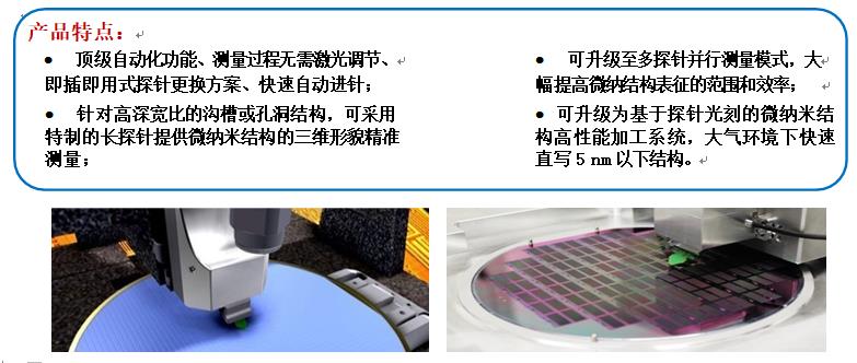
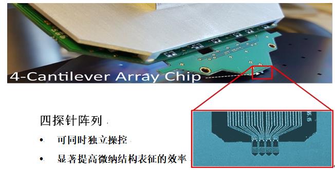
基于全球独 家利的、源自德国的主动式探针技术,百及纳米科技开发了下一代工业智能型原子力显微镜系统,针对工业域应用提供快速、智能的样品形貌表征,适用于工业型检错、质量评定和量化测量等,尤其适用于检测大尺寸晶圆或光学晶圆。
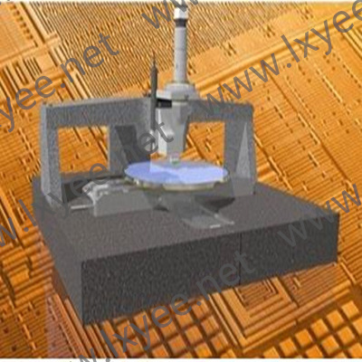
系统可集成大尺寸样品位移台、全自动光学导航系统和配套自动控制软件,可对大尺寸样品 进行全方位的光学成像定位,根据光学成像结果自动标定多个精确测量区域,并根据缺陷/待测结构的特点进行模式识别,智能选取原子力显微镜测量参数,在样品多个位置间自动移动,进行可 重复的高分辨率测量,生成检测书面报告,整个过程无需人工参与,终实现对大尺寸样品形貌 的智能化、自动化的高速、高效、高质量纳米测量。
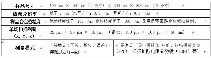
扫描结果示例:
扫描速率:6 mm/s
扫描范围:510mm x 135mm
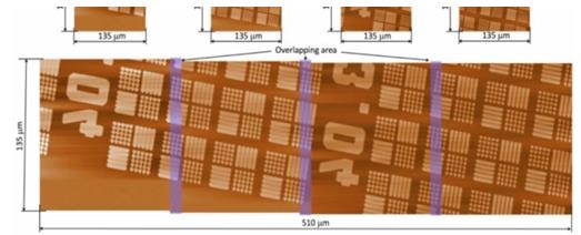
单次成像面积: 505 mm ×130 mm
结构高度: 60 nm
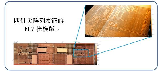
ParcanNano 100 nano industrial atomic force microscopy system
Based on the global patent home alone, from Germany active probe technology, best and nano science and technology to develop the next generation industrial system, intelligent atomic force microscope for industrial application provides a quick and intelligent the CLSM characterization, suitable for industrial inspection, quality evaluation and quantitative measurement of fault, especially suitable for detection of large size wafer or optical wafers.
System can be integrated displacement of large size sample machine, automatic optical navigation system and form a complete set of automatic control software, can be a full range of optical imaging of large size samples, according to the results of the optical imaging automatic calibration more accurate measurement area, and according to the characteristics of the defect/structures under test for pattern recognition, intelligent selection of atomic force microscope measurement parameters, It automatically moves between multiple locations of samples, carries out repeatable high-resolution measurements, and generates written test reports. The whole process requires no manual participation, and finally realizes intelligent, automated, high-speed, efficient and high-quality nanoscale measurement of large-size sample morphology.
热门标签:ParcanNano百及纳米原子力显微镜(工业型)