


当前位置: 阿仪网 > 光学仪器 > 光学仪表 > 其他 > 上海屹持光电技术有限公司 > 产品展示 > 光学元器件 > 测量和记录温度的镜片 > 硅镜片用于红外物镜Silicon Elements for IR Objective Lenses
硅镜片用于红外物镜


价格:¥ 电议
品牌名称:$brandModel.Title型号:Silicon Elements for IR Objective Lenses 原产地:中国大陆 更新时间:2026/9/21 7:50:14



支付方式:
- 支付宝 微信 银行转账
产品完善度: 访问次数:641
太赫兹设备
太赫兹器件
- 太赫兹晶体
- 太赫兹光电导天线
- 太赫兹近场探针
- 太赫兹透镜
- 太赫兹偏振片
- 太赫兹波片 THz waveplate
- 太赫兹滤波片 THz filter
- 太赫兹衰减片
- 太赫兹反射镜
- 太赫兹窗口片
- 太赫兹分束镜
- 太赫兹光栅
- 太赫兹棱镜
- 其他太赫兹元件
飞秒激光器
- NKT飞秒光纤激光器
- 飞秒再生放大器
- AVESTA飞秒光纤激光器
- 1um高重频飞秒激光器
- 飞秒超连续谱光源
- 飞秒光学参量振荡器OPO
- 钛宝石飞秒振荡器
- 光学频率梳
- 780/1560nm光纤飞秒激光器
- 掺Yb高能量高功率飞秒激光器
- 光纤飞秒放大器
- GHz高重频光纤飞秒激光器
- 2-3um中红外飞秒激光器
- 1.2um飞秒激光器
- TW太瓦飞秒放大系统
- 光学参量放大器OPA
皮秒激光器
- 皮秒光纤激光器
- Kanata皮秒激光器
- DPSS固态皮秒激光器
- 半导体皮秒激光器
- 高功率皮秒激光器
- 皮秒超连续谱激光器
- 可调谐皮激光器OPO
- Microchip微片皮秒激光器
- 高重频固态锁模皮秒激光器
- 高功率窄线宽皮激光器
- 高能量皮秒激光器
传统激光器
激光调制与测量
超快调制与测量
- CFBG啁啾光纤光栅
- 脉冲展宽器脉冲压缩器
- 半导体可饱和吸收镜SESAM
- 脉冲选择器
- 谐波产生倍频器
- 其他超快调制与测量
- 超快激光同步器
- 自相关仪
- 超短脉冲测量仪FROG
- 超快激光镜片
- 光子晶体光纤
- 超快激光压缩光栅
光谱影像
光纤通信与传感
光学元器件
镀膜与加工
X射线
磁克尔综合测试平台
半导体参数分析仪
光纤飞秒激光器
企业档案
会员类型:标准版
已获得阿仪网信誉 等级评定
(0 -40)基础信誉积累,可浏览访问
(41-90)良好信誉积累,可接洽商谈
(91+ )优质信誉积累,可持续信赖
阿仪网标准版会员:4年
工商认证 【已认证】

最后认证时间:
注册号: 【已认证】
法人代表: 【已认证】
参观次数:326524
详细内容
Silicon Elements for IR Objective Lenses
资料下载:Download Silicon Elements for IR Objective Lenses Datasheet (PDF, 144 KB)
TYDEX produces a wide range of elements made of silicon. We ensure strong control on every step of element production, from material selection to the measurement of obtained parameters of polished elements and coating characteristics. That is especially important in the manufacturing of precision imaging systems. This type of approach to the production of a set of large silicon optics for IR objective is described below.
The objective is intended for operating in two middle IR bands: 1.6 - 3.0mm and 3.5 - 5.5 mm. Its design incorporates 17 elements: 14 meniscus and plano-convex lenses with diameters from 10 mm to 210 mm and 3 plates with dimensions to 134 x 198 mm.
When manufacturing such multi-element imaging devices two important points should be taken into consideration: transmittance of the whole system and image distortion. These parameters depend on material quality (i) and surface accuracy (ii). Below we discuss our approach to control of these parameters (we will not touch the third critical point - coating parameters).
Material selection and control
For imaging systems the right choice of material is of utmost very importance. Defects in the material can cause image distortion and violate the system operation. This is the reason why so much attention is paid to selecting the material and its control. To provide the proper quality of material, silicon ingots with special parameters (dislocation-free optical grade monocrystalline Cz-Si with high homogeneity and transparency in the working range) were grown. After a few required ingots with diameter to 219 mm were ready the quality of material (resistance homogeneity, dislocation density, transmittance in the working range) is being controlled on samples prepared from each ingot. The typical transmission curve is presented here.
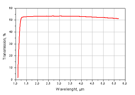
Fig. 1 Silicon transmission in the 1.1 - 5.7 mm spectral range. Sample thikness is 10 mm.
Surface accuracy control
As mentioned above, the second important parameter that should be considered is surface errors. Modern equipment allows to carry out complete interferometric control of a the whole surface or any part of it. Computer data processing enables us to obtain detailed information about different kinds of errors: regular errors (astigmatism, zonal error, coma), local errors, peak-to-valley value etc. In addition, representation of errors becomes easy to interpret.
For interferometric control Fizeau scheme is applied, λc = 632.8 nm (HeNe laser line). Additional equipment such as telescopic expanders and measuring objectives is used if required by surface shape and radius of curvature. Evaluation of the form error of a surface is being carried out in phase mode by means of measuring the deformation of the wavefront reflected from the controlled surface compared to test reference surface. Specialised integrated software is used to create phase data arrays and their further power polynomial approximation for surface error calculations.
Here we present as examples the results of such control for 2 surfaces: 1 - concave surface of meniscus D210 mm lens, and 2 - plane surface of 198 x 134 mm plate.
Interferometric measurements of errors of meniscus lens D210 mm
| concave R = -206.99 clear aperture - central D206 microns sphere |
| D= .080 | LX= 2.839 | LY= -.013 | C= 2.829 | RMS(W)= .031 | |
| A= .050 | FIA= .354 | RMS(W-A)= .023 | FA= .442 | ||
| B0= -.025 | RZ= .037 | ||||
| RMS(W-Z)= .029 | FZ= .131 | ||||
| B2= .149 | |||||
| B4= -.149 | |||||
| C= .110 | FIC= 164.892 | RMS(W-C)= .028 | FC= .178 | ||
| R= .139 | RMS(M)= .015 |
| RMS | MIN | MAX | R | STRL | STRH |
| .031 | -.144 | .092 | .237 | .964 | .988 |
| X : | -1.000 | .000 |
| Y : | .000 | -1.000 |

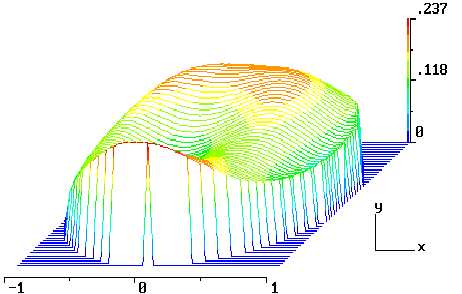
Fig. 2 Reconstracted wavefront topography presented at planar and 3-d plots.
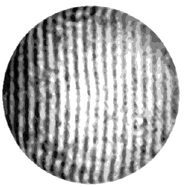
Fig. 3 Interferogram of the surface.
Interferometric measurements of errors of plane parallel plate 198x134 mm
The surface undergoes measurements in 2 areas: center zone of dimensions 70 x 70 mm (approximately the area occupied by incident ray) and the whole aperture 194 x 130 mm.
| plane R = infinity 70 x 70 microns plane |
| D= .000 | LX= 1.447 | LY= .033 | C= .964 | RMS(W)= .014 |
| A= .045 | FIA= 82.986 | RMS(W-A)= .010 | FA= .489 | |
| B0= -.014 | RZ= .023 | RMS(W-Z)= .012 | FZ= .235 | |
| B2= .064 | ||||
| B4= -.045 | ||||
| C= .012 | FIC= 173.740 | RMS(W-C)= .014 | FC= .009 |
| R= .076 | RMS(M)= .007 |
| RMS | MIN | MAX | R | STRL | STRH |
| .014 | -.035 | .044 | .079 | .993 | .998 |
| X : | -.680 | .680 |
| Y : | .680 | -.680 |
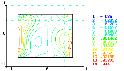
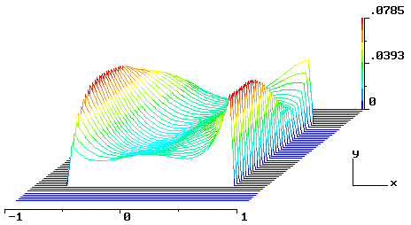
Fig. 4 Reconctracted wavefront topography presented at planar and 3-d plots.
| 194 x 130 microns plane |
| D= .000 | LX= 2.811 | LY= .053 | C= 2.045 | RMS(W)= .024 | |
| A= .104 | FIA= 81.477 | RMS(W-A)= .011 | FA= .787 | ||
| B0= -.020 | RZ= .083 | RMS(W-Z)= .016 | FZ= .561 | ||
| B2=.039 | |||||
| B4= .117 | |||||
| C= .022 | FIC= 50.186 | RMS(W-C)= .023 | FC= .014 |
| R= .077 | RMS(M)= .012 |
| RMS | MIN | MAX | R | STRL | STRH |
| .024 | -.036 | .076 | .112 | .978 | .993 |
| X : | -.200 | .680 |
| Y : | .480 | -.440 |
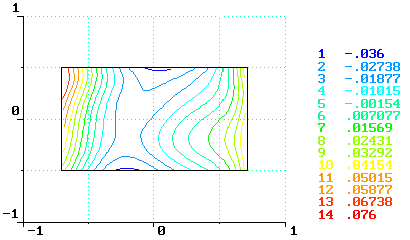
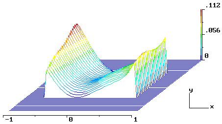
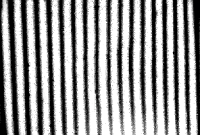
Fig. 6 Interferogram of the surface S1.
Such thorough control on each step of production can guarantee that all parameters of the item meet specifications required by customer and that the device will operate in a proper way.
热门标签:硅,Si,红外物镜